AR coatings
  HR coatings
  Stresses
  Mid-infrared dispersive mirrors
Notch filters
Notch filters are used to reflect or block a a narrow spectral range (stop band) and to transmit relatively broad range around the stop band. Thin-film notch filters are commonly used in optical applications such as fluorescence microscopy, spectrophotometry, and laser systems [1], [2], [3], [4], [5]. They can be designed to have very high precision and accuracy, with narrow stop bands and steep edges.
For notch filter designing, the following key specifications are important:
- Central wavelength; very often the central wavelength of notch filters is called the laser line:
- Stop band width or the width of the high-reflection zone around the central wavelength;
- Overall transmittance level in the high transmittance (low reflectance) range;
- The specification at the central wavelength can be (1) a peak reflectance in a.u. or in % or (2) the transmittance in optical density (OD).
The design structure of a thin-film notch filter is strongly dependent on the key desired properties - the width of the high reflection zone (HR) and the peak reflectance. The higher the peak reflectance that is desired, the larger the total thickness of the filter and the number of layers required.
In Fig. 1, reflectance of two notch filter designs are shown: a 52-layer design with the refractive index profile presented in Fig. 3 and a 70-layer design. It is easily to see that the 70-layer design provides steeper edges, which means that it provides a sharper transition between the high reflection and high transmittance regions. In vicinity of the laser wavelength of 1030 nm, the peak reflectance data are not distinguishable in this scale.
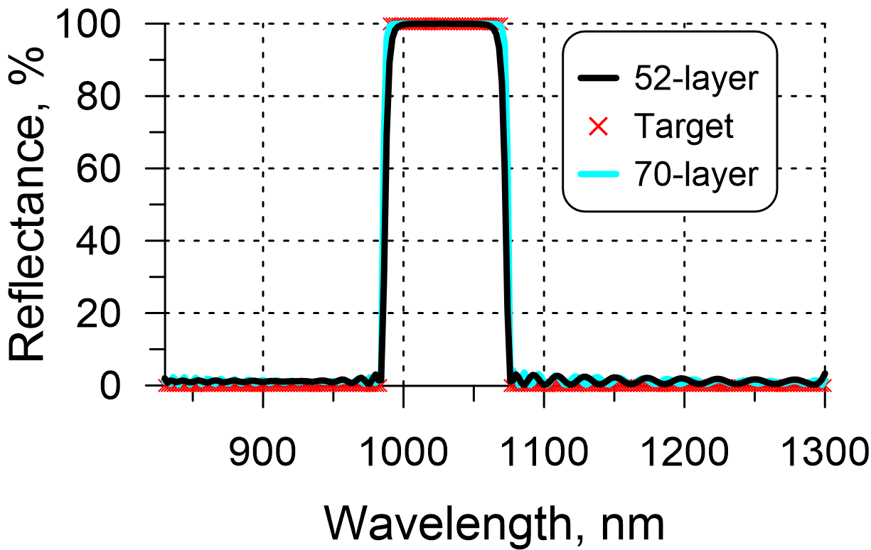
Fig. 1. Reflectance of a 52-layer (Fig. 3) and a 70-layer notch filter designs.
The optical density (OD) is a measure of the attenuation or blocking ability of a notch filter to block or attenuate specific wavelengths of light:
$$ OD=-\log_{10}(T) $$
In order to analyze the filter characteristic at the laser wavelength in more detail, the transmittance curves of both filters in OD are plotted in Fig. 2. The thicker 70-layer notch filter exhibits higher OD (>6.5) than the thinner 52-layer filter (OD is about 4). This means that the thicker filter is more effective at blocking or attenuating the laser wavelength than the thinner filter. On the other hand, production of the 70-layer filter is more complicated because of stronger accumulation of deposition errors.
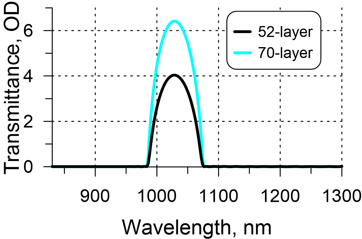
Fig. 2. Transmittance in OD of a 52-layer (Fig. 3) and a 70-layer notch filter designs.
The notch filters exhibit very often a characteristic pattern (see example in Fig. 3): they consist of very thin and very thick layers. The structure shown in Fig. 3 resembles a periodic structure close the one that can be specified by a formula: $ (0.14 H\; 3.86 L)^{26} $, where $H$ and $L$ denote quarter-wavelength thicknesses of high- and low-index materials. The H-index layer thicknesses are modulated around the average value of 0.14 and the L-index thicknesses are modulated around the value 0.86. The sum of thicknesses of two neighboring layer is close to 4.
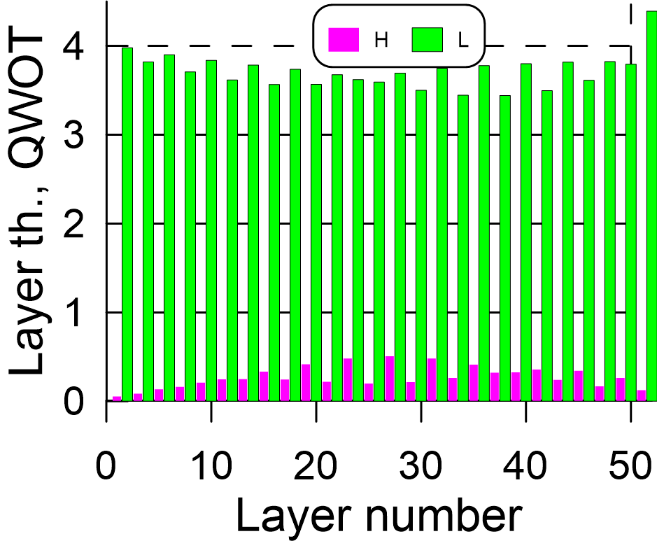
Fig. 3. Struture of a 52-layer notch filter design.
- Of course, notch filter design structures and their main characteristics are dependent on layer materials and the substrate as well.
- Notch filters can be designed using some types of periodic structures as starting designs. These structures are:
$$ S1:\qquad\qquad \left(p n_1\; (2-p) n_2\right)^m, $$
$$ S2: \qquad\qquad \left(p n_1 \; (4-p) n_2 \right)^m, $$
where $n_1$ and $n_2$ are quarter-wave layers of high- and low-index thin-film materials (for example, $n_1$ is H-index material and $n_L$ is L-index material or vice versa); $m$ is the number of layer pairs. The parameter $p$ is between 0 and 1. This parameter defines the ratio between H- and L-layer thicknesses. With $p=1$, the S1 structure is a quarter-wave mirror.
There are some interesting qualitative and quantitative conclusions from these analytical estimations:
- As the total thickness is a conservative parameter, it is possible to estimate in advance the number of layers and their thicknesses required to achieve a specified peak reflectance. This estimation can be done by analytical formulas [6] related to S1 and S2 structures.
- Interesting: It follows from these analytical estimations that the width of the HR zone (blocking range) depends on the structure (S1 or S2) and does not depend on the number of layers. The width of the HR zone for S1 structures is two times broader than the bandwidth of the corresponding S2 structures. Of course, the total thickness of the S2 structures is about two times larger than the total thickness of the corresponding S1-designs.
- It is interesting that peak reflectance of S1 and S2 structures are the same.
- Therefore, it looks like that the S1 structures are more attractive since they are thinner and do not contain ultra-thin and ultra-thick layers. It is actually not so. The HR zone of the S1 structure is limited, and this limit is defined by the $p$ value: the smaller the $p$-value, the narrower the HR zone. Practically, the $p$-value that corresponds to the thinnest layer cannot be very low. If your blocking range is very narrow, the S2 structure should be used.
- The peak reflectance is dependent not only on the structure and the $p$-value but is dependent essentially on the number of layer pairs $m$.
- Using our Notch Filter Calculator, you can try by yourself. You can simply input refractive indices $n_1$, $n_2$, and $n_s$ (refractive index of the substrate), the $p-$ fraction, and the number of layer pair $m$. You will see the width of the HR zone (blocking range), the refractive index profiles in the case of S1 and S2 structures, and the transmittance in OD vs. $m$.
References:
[1] A. Thelen, Design of Optical Interference Coatings (McGraw-Hill, 1988).
[2] K. D. Hendrix et al., Demonstration of narrowband notch and multi-notch filters, Proc. SPIE 7067, Advances in Thin-Film Coatings for Optical Applications V, 706702 https://doi.org/10.1117/12.795498
[3] L. Young, Multilayer Interference Filters with Narrow Stop Bands, Appl. Optics Vol. 6, pp. 297-315 (1967) https://doi.org/10.1364/AO.6.000297
[4] M. Scherer et al., High performance notch filter coatings produced with piad and magnetron sputtering, Proc. SPIE 7101, 71010I (2008) https://doi.org/10.1117/12.797699
[5] U. Schallenberg et al., Design and manufacturing of high-performance notch filters, Proc. SPIE Vol. 7739, 77391X (2010) https://doi.org/10.1117/12.856580
[6] T. Amotchkina, Analytical estimations for the reference wavelength reflectance and width of high reflection zone of two-material periodic multilayers, Appl. Opt., Vol. 52, pp. 4590-4595 (2013) https://doi.org/10.1364/AO.52.004590