With OTF Studio Software, you can tackle multilayer design challenges of any complexity. It offers powerful design and analysis tools, including synthesis algorithms enhanced with machine learning elements.
For trial versions, please reach out to our distribution partners.
Anti-reflection coatings
- Anti-reflection coatings (AR) are used to minimize the Fresnel reflection of a surface in a certain wavelength range. Due to Fresnel reflection, a transmittance of an uncoated glass substrate in the visible range is about 92% (4% of light is reflected from each substrate). A 6-layer AR coating allows you to reduce reflectance down to 0.3%.
- AR coatings can be used in camera lenses, optical windows, display screens, photovoltaic solar panels, automotive displays, architecture glass, eye glasses, etc.
- AR coatings in optical systems increase transmittance, enhance contrast, remove back-side reflectance, and prevent appearance of ghost images.
- AR coatings are demanded also in laser systems to reduce back-side reflectance that can destabilize laser beams and deform laser pulses: they can be deposited on the substrate back side to compensate stresses caused by front side coatings and prevent thermal lensing in laser setups.
- There are many types of AR coatings, among them are single-wavelength AR coatings ("V" AR coatings), double-wavelength AR coatings ("W" coatings), narrow-band AR coatings, broadband AR coatings, dual- and triple-band AR coatings, omnidirectional AR coatings, combined AR coatings, etc.
OTF Studio® Thin Film software solves all AR design problems fast and effective.
Watch our YouTube videos to explore real-time demonstrations of antireflection coating designs:
- Dual-Band Antireflection Design
- Antireflection coating for the visible spectral range
- Omnidirectional AR coating
- Designing a Mid-Infrared Anti-Reflection Coating with OTF Studio
- Triple-Band Anti-Reflection Multilayers
- Designing Single and Dual-Wavelength Anti-Reflection Coatings with OTF Studio Thin-Film Software
"V" and "W" AR coatings
Single-wavelength AR coatings provide zero reflectance at a certain target wavelength. Single-wavelength AR coatings (so called "V" coatings) consist of two layer only (see Fig. 1). Of course, in order to produce such coatings with high accuracy, an accurate monitoring process is required. Even small errors in layer thicknesses can lead to shift of coating reflectance and therefore significant deviation of the experimental reflectance from zero at the target wavelength.
In Fig. 1 (left) theoretical reflectance of an 2-layer AR coating is shown by black curve. Two other curves show reflectance data of the same design with disturbed layer thicknesses (errors of 1% level). It is seen that even such small errors can lead to strong deviations from the target reflectance.
It is recommended to design and produce 4-layer AR, which are more stable to deposition errors and provide almost zero reflectance in the vicinity of the target wavelength (Fig. 2, right panel). Such solutions provide a flat reflectance around the target wavelength.
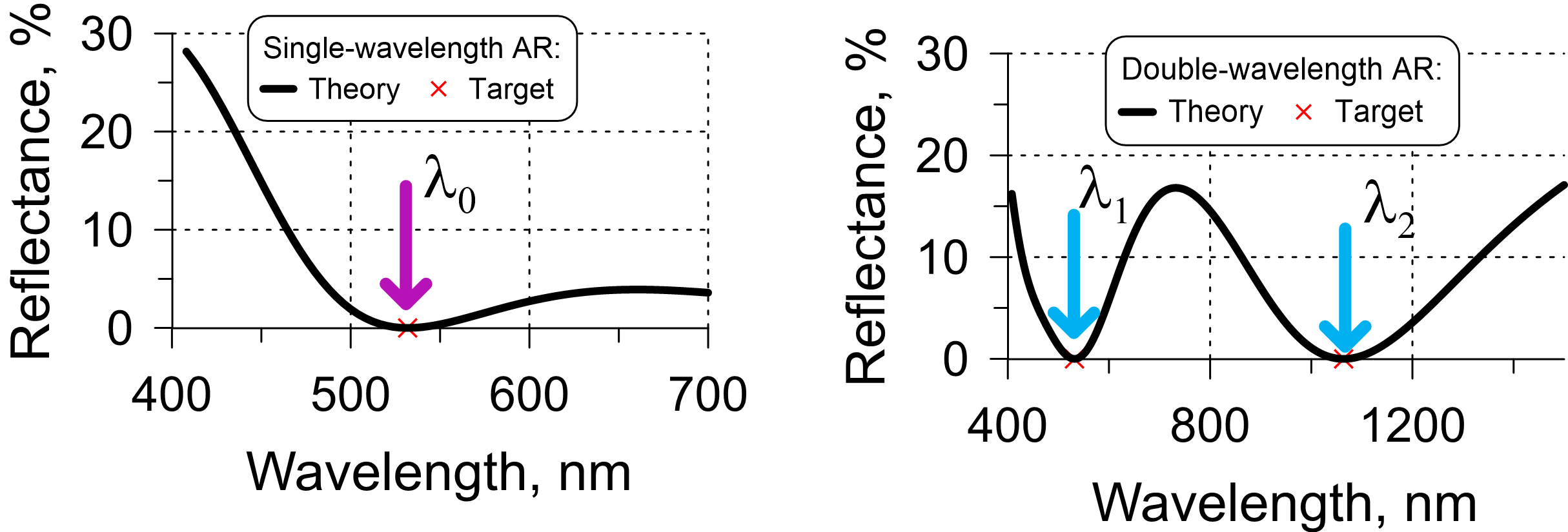
Fig. 1. Left: Target (one wavelength point 532 nm) and theoretical reflectance of a two-layer AR coating; Right: target (two wavelength points 532 nm and 1064 nm) and theoretical reflectance of a 4-layer AR. coating.
In Fig. 2 (right), the black curve indicates theoretical reflectance of a 4-layer design and the orange curve shows theoretical curve of the design with errors in layer thicknesses of 1.5% level. The curve shifted but the target reflectance is achieved. 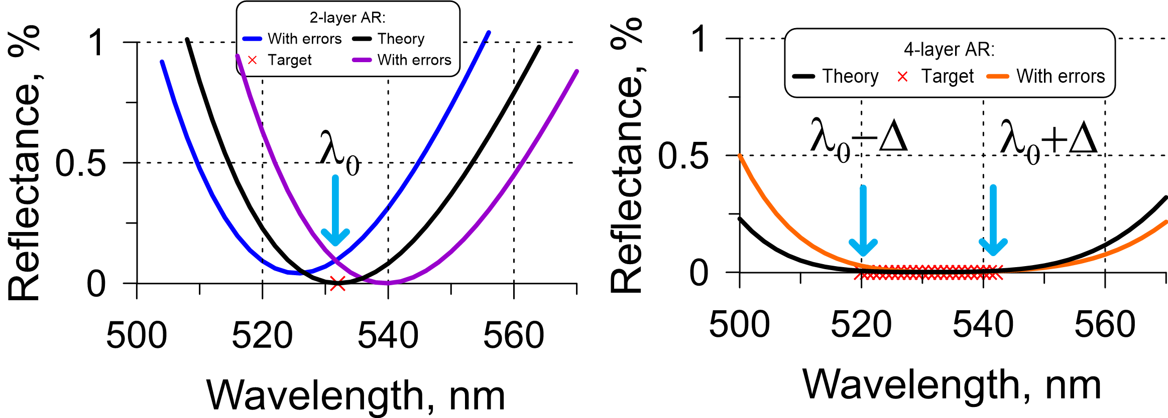
Fig. 2. Left: Target (one wavelength 532 nm), theoretical reflectance of a two-layer AR coating, and two reflectance curves corresponding disturbed designs ith 1% level errors; Right: target (532 nm \(\pm\) 10nm), theoretical reflectance of a 4-layer AR. coating, and reflectance curve corresponding to a disturbed design with 1.5% level of errors.
"W" AR coatings
In double-wavelength AR coatings (so called "W" coatings), reflectance at two wavelengths is zero (Fig. 1, right). For this purpose, 4-layer solutions can be easily found. As in the case with single-wavelength AR coating, it is recommended to minimize the reflectance not at two target wavelength points (as in Fig. 1, right panel) but in the vicinity of these wavelengths in order to increase coating stability to deposition errors.
Learn more in our YouTube video Designing Single and Dual-Wavelength Anti-Reflection Coatings
Dual-band anti-reflection coatings
Dual-band AR coatings provide minimum reflectance in two spectral ranges of interest (target spectral ranges). Such coatings are often used in laser setups and designed for bandwidth of two laser wavelengths. Fig. 3(left panel) plots theoretical reflectance of an example 8-layer AR design shown in the right panel (Fig. 3). The AR design exhibits minimum reflectance in the range from 500 to 600 nm and from 950 to 1100 nm covering bandwidths of laser wavelengths of 532 nm and 1064 nm, respectively.
Dual-band AR coatings are very demanded in mid-infrared spectral ranges, for example, in the regions 3-5 \(\mu\)m and 8-12 \(\mu\)m.
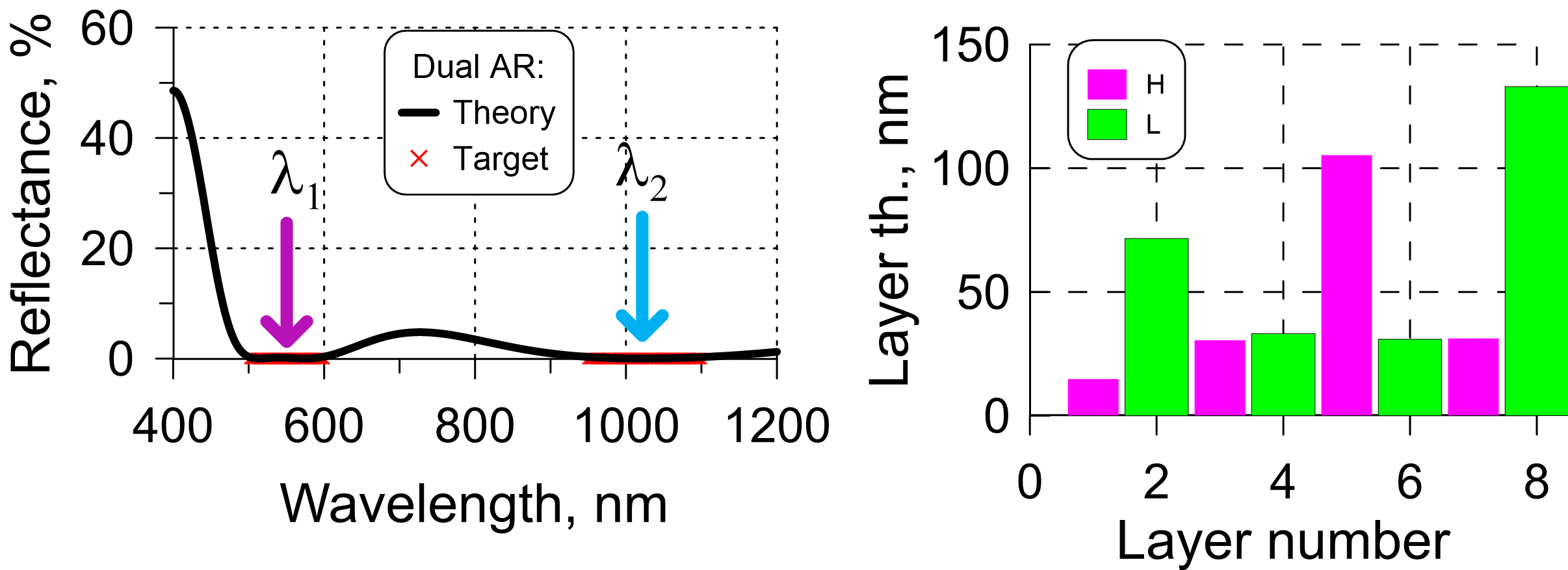
Fig. 3. Left: Target (reflectance is zero in the ranges 500-600 nm and 950-1100 nm), theoretical reflectance of a 8-layer AR coating; design structure of the 8-layer solution.
Learn more in our YouTube video Designing Dual-band AR coating with OTF Studio.
Triple-band AR coatings
Triple-band AR coatings exhibit lowest reflectance in three spectral bands. In Fig. 4, spectral characteristics and the design structure of a 16-layer solution are shown. The design exhibit lowest reflectance in the spectral ranges 340-390 nm, 550-750 nm, and 1350-1650 nm covering vicinity of typical laser wavelengths of 360 nm, 633 nm, and 1550 nm. 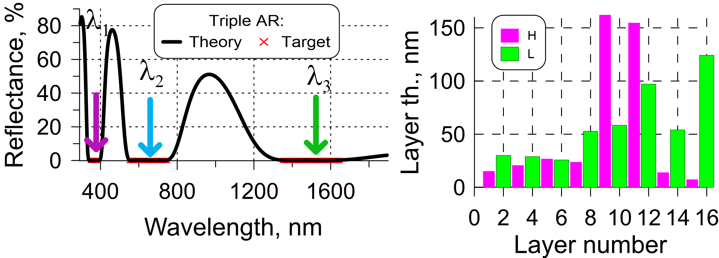
Fig. 4. Left: Target (reflectance is zero in the ranges 340-390 nm, 550-759 nm, and 1350-1650 nm), theoretical reflectance of a 16-layer AR coating; Right: design structure of the 16-layer solution.
Learn more in our YouTube video Designing triple-band AR coating with OTF Studio.
Broadband AR coatings
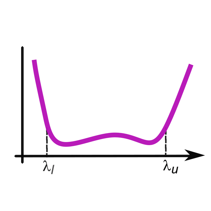
We refer to AR coatings as to broadband ones, if the ratio of lower and upper boundaries of the AR spectral range is larger than 2. For example, AR operating in the range 400-800 nm is broadband. Even using the most effective design algorithms it is not possible to achieve residual reflectance low than a minimum residual reflectance value \(R_{res}\). This \(R_{res}\) value is dependent of AR design problem parameters: layer refractive indices \(n_H\) and \(n_L\), substrate refractive index \(n_s\), and ratio of the boundaries of the AR operating range \(\lambda_l\) and \(\lambda_u\) (Fig. 5, left panel).
Of course, in the case of oblique incidence AR coatings, the incidence angle AOI plays an important role. For large AOI, residual reflectance grow, especially for AOI exceeding 60°.
Reflectance of a 16-layer broadband AR coating designed for the spectral range 400-2000 nm and the structure of this coating are plotted in Fig. 5 (ratio of the upper and lower boundaries of the AR range is 5).
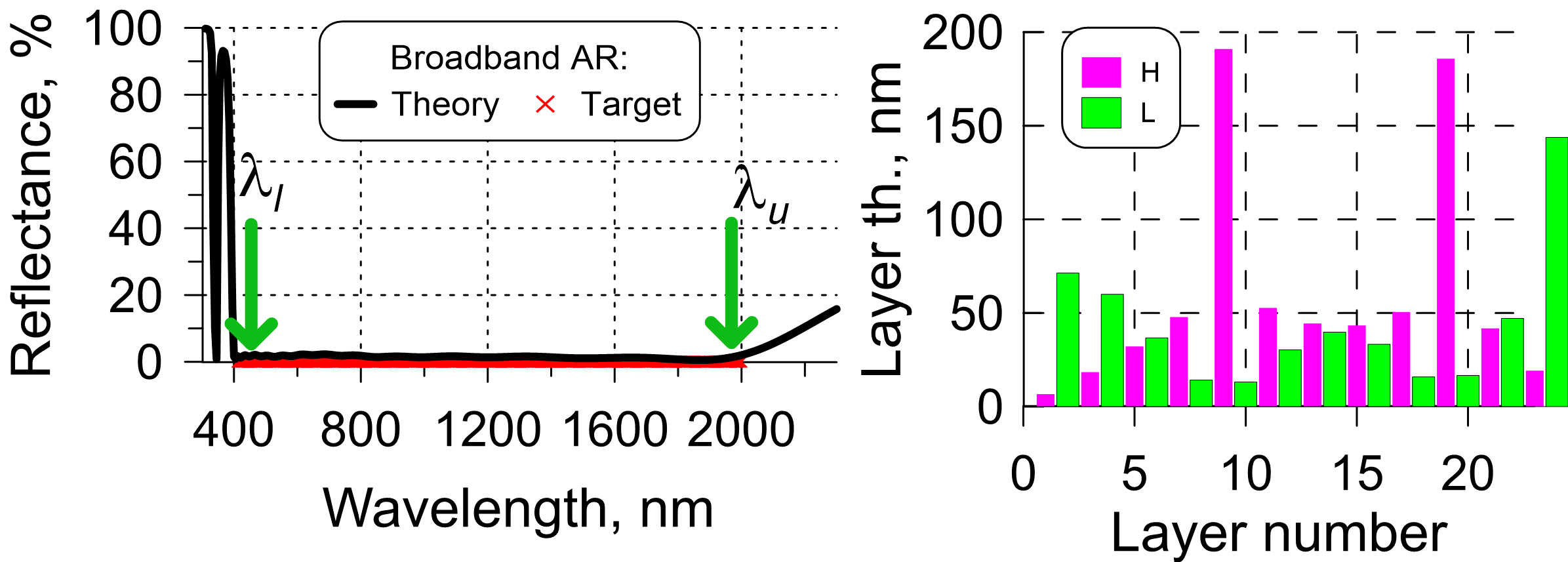
Fig. 5. Left: Target (reflectance is zero in the range 400-2000 nm), theoretical reflectance of a 16-layer AR coating; Right: design structure of the 16-layer solution.
If you are interested, you can find the estimations of the minimum achievable reflectance in our AR calculator. These estimations are especially useful for AR coatings in the mid-infrared spectral range, where it is difficult to achieve low residual reflectance values since refractive indices of typical substrates like Ge, Si, ZnSe are high.
Learn more in our YouTube video Antireflection coating for the visible spectral range
Combined AR coatings
AR coatings can be design for a large combination of spectral ranges: operating spectral ranges can consist of multiple narrow and wide bandwidths. In Fig. 6, an example for a combined AR coating is shown: the 12-layer AR design (right panel) provides lowest reflectance in a narrow spectral range from 1000 to 1060 nm (in the vicinity of the Yb:YAG laser wavelength of 1030 nm) and in a broad range from 1500 to 2700 nm. 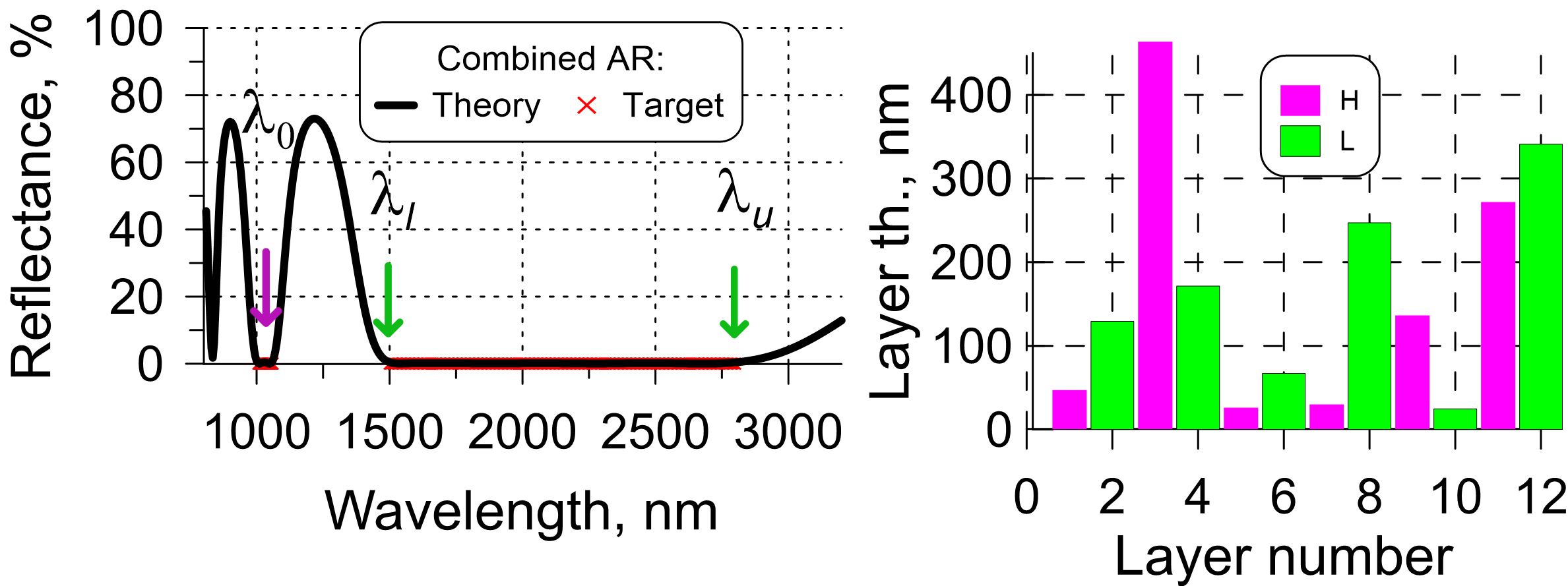
Fig. 6. Left: Target (reflectance is zero in the ranges 1000-1060 nm and 1500-2700 nm), theoretical reflectance of a 12-layer AR coating; design structure of the 12-layer solution.
AR coatings for oblique light incidence
AR multilayers solution for oblique incidence case or for a certain angular range can found for narrow and broadband spectral ranges and for s-, p-, and average polarization states. The larger the angle, the higher is residual reflectance. Even with the most effective and sophisticated design algorithms, it is not possible to reduce reflectance at large AOI significantly. This is true not only for an angular range but also for a single AOI (for example, 70-75°).
You can experiment with estimations in our calculator for broadband AR coatings and s-polarization case.
In the example below (Fig. 7), reflectance of an 16-layer AR design for the visible range is shown. The design is operating from 0° to 60°; the light is not polarized. It is seen that the curve corresponding to 60° is significantly higher than reflectance values corresponding to other angles. 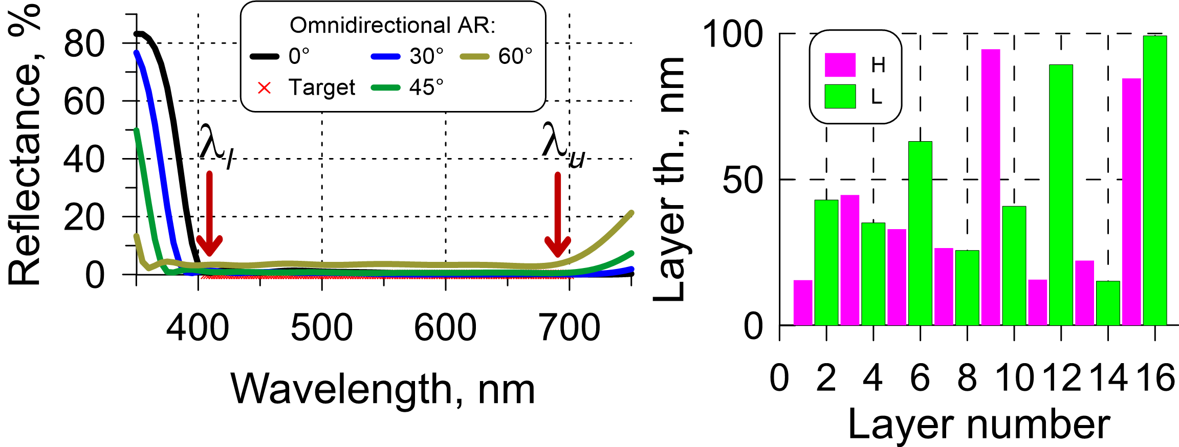
Fig. 7. Left: Target (reflectance is zero in the visible range and for incidence angles from 0° to 60°) and theoretical reflectance of a 16-layer AR solution; Right: design structure of the 16-layer multilayer design.
Learn more in our YouTube video Omnidirectional anti-reflection coatingLearn more in our YouTube video Omnidirectional anti-reflection coating
AR Coatings for different environments
It may happen that coatings (very often AR coatings) are deposited on large surfaces or on curved surfaces (domes, lenses). Due to technological reasons, layer thicknesses at different points on the deposited sample can be different (see a sketch in Fig. 8, left panel). It means that an AR design should approximate target reflectance at any point of the sample.
Example: a target from Fig. 6 is considered: anti-reflection coating should operate in the vicinity of the Yb:YAG laser wavelength of 1030 nm and in the broadband spectral range from 1500 nm to 2700 nm. Imagine that we deposit this design on a lens and we know that due to technological reasons, there is thickness inhomogeneity by radius at different distances from the center. It is known that correction factors of layer thicknesses in positions \(x_1\) and \(x_2\) of high-index material is \(CorrH_1=0.9\) and \(CorrH_2=0.95\), respectively, and correction factors in positions \(x_1\) and \(x_2\) of the low-index material are \(CorrL_1=0.94\) and \(CorrH_2=0.88\). It means that in positions \(x_1\) and \(x_2\), instead of the layer thickness d that we expect at the central position \(x_0\), we obtain \(d_1=CorrH_1\cdot d\), \(d_2=CorrH_2\cdot d\) for high-index material and \(d_1=CorrL_1\cdot d\), \(d_2=CorrL_2\cdot d\) for low-index material. An 8-layer AR design solution exhibit reflectance curves shown in Fig. 8 (right panel): black curve shows reflectance at the central position; blue and green curves show reflectance values at radial positions \(x_1\) and \(x_2\).
Generally, it is more difficult to find a good design for large deviations of correction factors from 1. 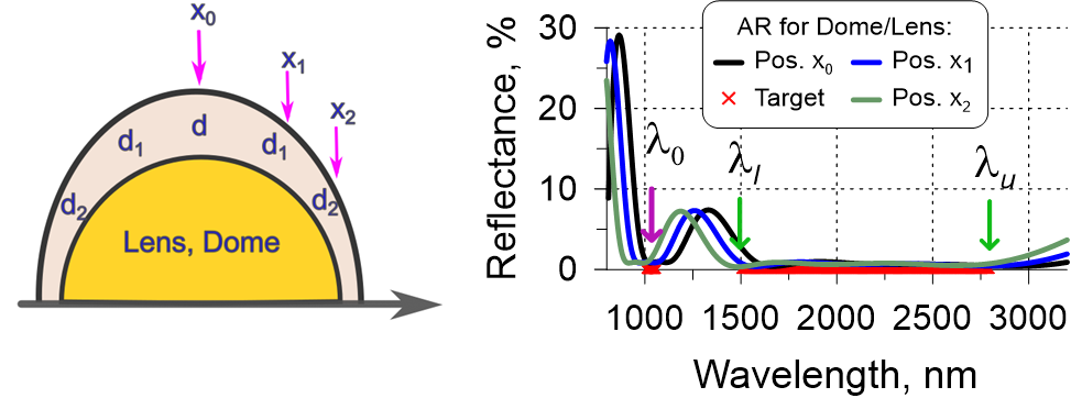
Fig. 8. Left: Target (reflectance is zero in the ranges 340-390 nm, 550-759 nm, and 1350-1650 nm), theoretical reflectance of a 16-layer AR coating; design structure of the 16-layer solution.
There are other situations when you need one AR design for multiple environments, for example:
- If you need to design and produce the same AR design for crystals (all surfaces) in one deposition run;
- If you have mass production and need to manufacture one design for various substrates at the same deposition run;
- If you need to take into account thermal effect and your coatings are supposed to operate at different temperatures;
- If you will use the same design in the air and in other media (for example, water or another liquid).
Stress-compensating AR coatings
Coating layers have residual mechanical stresses. After summing up stresses from all coatings layers, the resulting stress is can be high enough to bend/deform even thick substrates. This is very critical for laser applications where even a small deformation of an optical component can lead to distortion of the laser beam. To prevent this effect, an AR coating can be deposited on the back-side of the substrate. Also, together with stress compensation, the unwanted reflections from the back side will be suppressed.
Example: Assume that a quarter-wave mirror at 1030 nm (QWM @ 1030) is deposited on the substrate front side. The mirror contains 15 layers of high- (H) and low (L)-index materials; the total QWM thickness is 2120 nm; the total thickness of H-layers is \(\Sigma_H=877 \) nm and the total thickness of L-layers is \(\Sigma_L=1243\) nm. The HR zone of the QWM is from 950 nm to 1200 nm. In order to compensate the stress and to exclude the back side reflectance, an AR coating should be deposited on the back side. For the range 950-1200 nm, a four layer AR would provide low reflectance (see Fig. 9). The total thickness of the coating is \(\Sigma=431\) nm that is \(\Sigma_H=218 \) nm of H material and \(\Sigma_L=213\) nm of L material. These thicknesses do not compensate stress caused by the QWM coating (you can estimate stresses here). To compensate the stress of the front side, the total thicknesses of H- and L-material in the AR design should be very close to the corresponding total thicknesses of the QWM design.
A 14-layer AR design with spectral performance shown in Fig. 9 provides H-layer thicknesses of \(\Sigma_L=1236\) nm and L-layer thicknesses of \(\Sigma_L=884\) nm. The stress resulting from the both sides is therefore almost zero. Of course, production of 14-layer AR design is more complicated that the production of the simple 4-layer design. 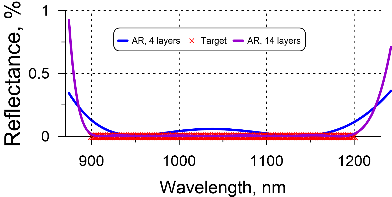
Fig. 9. Comparison of spectral performances of a standard 4-layer AR design and a 14-layer AR design compensating residual stress caused by the QWM @ 1030 mirror.
If your deposition process provides high monitoring accuracy, even more complicated ARs can be easily produced. For example, in this paper, we report about design and production of a 71-layer AR with the total thickness of 7.5 um compensating stress caused by a 74-layer dispersive mirror multiterawatt for few-cycle light wave synthesizer based on optical parametric amplification.
If you are interested in our assistance in designing AR and other types of coatings, please contact us! We can design for you or we can send you a design that will be a good starting point for your design process. We have many years of experience in thin film optics.
If you have questions, please ask per e-mail or phone us. ZOOM or Teams meetings are also possible.
Further reading:
- T. Amotchkina, Empirical expression for the minimum residual reflectance of normal- and oblique-incidence antireflection coatings, Appl. Optics Vol. 47, pp. 3109-3113 (2008) https://doi.org/10.1364/AO.47.003109
- T. Amotchkina, M. Trubetskov, V. Pervak, A. Tikhonravov, Design, production, and reverse engineering of two-octave antireflection coatings, Appl. Opt. Vol. 47, pp. 3109-3113 (2008) https://doi.org/10.1364/AO.47.003109
- T. Amotchkina, A. Tikhonravov, M. Trubetskov, Estimation for the number of layers of broad band anti-reflection coatings, Proc. SPIE 7101, 2008, https://doi.org/10.1117/12.796590
- V. Janicki, S. Wilbrandt, O. Stenzel, D. Gäbler, N. Kaiser, A. Tikhonravov, M. Trubetskov, T. Amotchkina, Hybrid optical coating design for omnidirectional antireflection purposes, J. Opt. A: Pure Appl. Opt. 7 (2005) L9–L12 doi:10.1088/1464-4258/7/8/L01
With OTF Studio Software, you can tackle multilayer design challenges of any complexity. It offers powerful design and analysis tools, including synthesis algorithms enhanced with machine learning elements.
For trial versions, please reach out to our distribution partners.
OTF Studio workshop is an excellent opportunity to learn more about its capabilities and gain hand-on experience.