AR coatings
  HR coatings
  Stresses
  Mid-infrared dispersive mirrors
Stresses in multilayer coatings
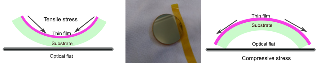
Fig. 1. Schematic of the tensite and compressive stress.
Stresses in thin films is an important issue affecting surface flatness. Stresses in coating layers can lead to delamination, cracks, buckling, spallations and reduce adhesion of the coatings. The stresses result from different thermal expansion coefficients of layer materials and substrates. Knowing stresses is important in many applications with respect to stability and durability of the optical elements. If you know stresses in your thin film materials $\sigma_H$ and $\sigma_L$ and total physical thicknesses of the layers of high and low-index materials $\Sigma_H$ and $\Sigma_L$, you can calculate the stress $\sigma$ of the multilayer design:
$$ \sigma=\frac{\Sigma_H\cdot \sigma_H+\Sigma_L\cdot \sigma_L}{\Sigma_H+\Sigma_L} Eq. (1)$$
Stresses in H- and L-layers in MPa: σH = MPa σL = MPa
Total thicknesses of H- and L-layers in μm: ΣH = μm ΣL = μmMechanical stresses in coatings layers is influenced by deposition technique and deposition parameters (see, for example, [1], [2]). Mechanical stress in the coating may be high enough to bend even a quite thick substrate. This can distort the beam wave front of the entire laser system. Poor mechanical properties of the coating layers can induce degradation of the optical properties of multilayers.
There are multiple publications studying stresses in thin films and optical coatings. Typically, the total mechanical stress includes three components: external, intrinsic, and thermal ones (see, for example, [1]).
For some design problems, it is important to know expected residual stress values in multilayer solutions. In this case, you can use the formula Eq. (1) based on Stoney formula [1]. To apply this formula, you need to know stresses $\sigma_H, \sigma_L$ in your layer materials. It is possible that these stress values are not close to the values reported in literature. These values can have even the opposite sign (i.e., your films exhibit tensile stress instead of compressive or vice versa).
How to estimate stresses $\sigma_H, \sigma_L$ in your thin film materials?
There are various methods of measuring stresses (see, for example, [1], [2]).
One of the possible methods to estimate the residual film stress is following. A relatively thick film can be deposited on a very thin (for example, 1 mm) substrate. Deflections of the coated substrate and uncoated substrates ($x$ and $x_s$, see Fig. 2) can be measured, for example, using a profiler. Having $x$ and $x_s$, the radii of curvature $R_1$ and $R_2$ (before and after the deposition) can be calculated using simple geometrical formulas. Then, residual stress can be estimated as:
$$ \sigma=\frac 16\cdot \left(\frac{1}{R_2}-\frac{1}{R_1}\right ) \cdot \frac{E d_s^2}{(1-\nu) d_f}, Eq. (2)$$
where $E$ is Young's modulus, $\nu$ is Poisson's ratio, $d_s$ is substrate thickness, $d_f$ is film thickness [1, 4].
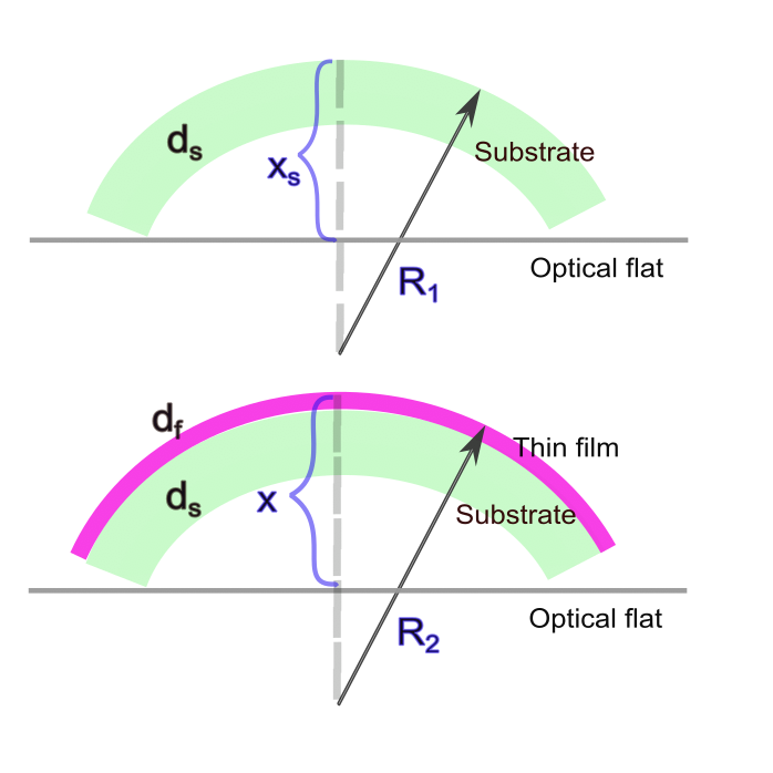
Fig. 2. Schematic representation of the measurement process: deflections of the uncoated substrate $xs$ (upper panel) and the coated substrate $x$ (lower panel) are measured using a surface profilometer. The radii $R_1$ and $R_2$ can be easily calculated knowing substrate diameter.
Deflections of uncoated and coated substrate $x_s$ and $x$: xs = nm x = nm
Young's modulus [GPa] and Poisson's ratio [a.u.] E = GPa ν =
Substrate thickness $d_s$ [mm], substrate diameter D [mm], and film thickness df [nm] ds = mm D = mm df = nm
For the calculations you need to know Young's modulus and Poisson's ratio. These values of various widely used substrates are plotted in Fig. 3. The data taken from open sources:
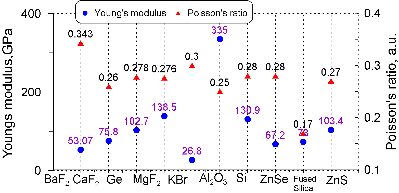
Fig. 3. Young's modulus $E$ and Poisson's ratio $\nu$ [5], [6].
Residual stresses in thin films depend on multiple factors including deposition technique, deposition parameters etc. Stress values of some typical thin-film materials used in the visible, near-infrared, and mid-infrared coatings are collected in the table below.
| Thin-film material | Deposition method | Stress* in MPa | Reference |
| TiO2 | Ion-beam assisted deposition | -540 | [2] |
| Al2O3 | Reactive ion platting | -210 | [2] |
| Ta2O5 | Radio frequency magnetron sputtering | -200 to 350 | [2] |
| SiO2 | -150 to -270 | [2] | |
| Nb2O5 | +100 to -1100 | [2] | |
| Al2O3 | -200 to -1200 | [2] | |
| Ge | E-beam evaporation (120°) | -50 | [8] |
| YbF3 | 140 | [8] | |
| LaF3 | 380 | [8] | |
| ZnS | -400 | [8] | |
| ZnS | E-beam evaporation (room temp.) | -350 | [9] |
*) Compressive stress - negative sign, tensile stress - positive sign.
References:
[1] A. E. Ennos, “Stresses Developed in Optical Film Coatings,” Appl. Opt. 5(1), 51–61 (1966) https://doi.org/10.1364/AO.5.000051
[2] G. N. Strauss, Mechanical stress in optical coatings, In: Kaiser, N., Pulker, H.K. (eds) Optical Interference Coatings. Springer Series in Optical Sciences, vol 88. Springer, Berlin, Heidelberg;
[3] H.A. Macleod, Thin-Film Optical Filters, 4th ed. (Taylor & Francis, 2010).
[4] S. Kičas, U. Gimževskis, and S. Melnikas, “Post deposition annealing of IBS mixture coatings for compensation of film induced stress,” Opt. Mater. Express 6(7), 2236 (2016) https://doi.org/10.1364/OME.6.002236
[5] https://www.thorlabs.com/newgrouppage9.cfm?objectgroup_id=6973
[6] https://ii-vi.com/product/zinc-sulfide-zns/
[7] T. Amotchkina, M. Trubetskov, M. Schulz, V. Pervak Comparative study of NIR-MIR beamsplitters based on ZnS/YbF3 and Ge/YbF3, Optics Express Vol. 27, pp. 5557-5569 (2019) https://doi.org/10.1364/OE.27.005557
[8] T. Amotchkina, M. Trubetskov, D. Hahner, V. Pervak, Characterization of e-beam evaporated Ge, YbF3, ZnS, and LaF3 thin films for laser-oriented coatings, Applied Optics Vol. 59, pp. A40-A47 (2020) https://doi.org/10.1364/AO.59.000A40
[9] C. de Vita et al., Room-temperature deposition of ZnS antireflection coatings for MIR-LWIR applications, Vol. 12, Optical Materials Express (2022). https://doi.org/10.1364/OME.439843